Ion Milling
Ion milling employs an ion beam to cut samples, without the need to molded the sample. This technique directly cuts the sample, creating a cross-section for detailed observation. This method effectively avoids the stress effects that may be caused by conventional mechanical grinding. Moreover, ion beam milling can also be used for precise polishing and surface cleaning, enhancing the quality of the observational results.
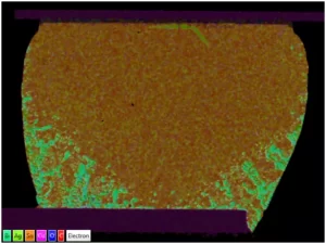
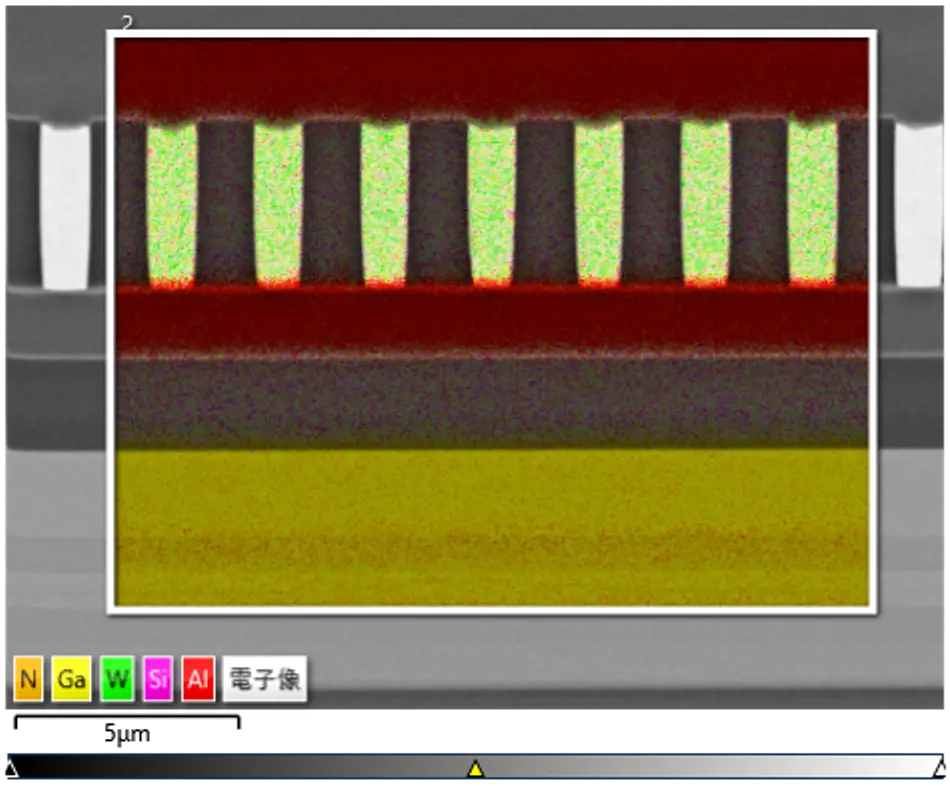
SEM, Scanning Electron Microscope
Scanning Electron Microscopy (SEM) operates by focusing an electron beam onto the surface of a sample, which in turn generates secondary signals like Secondary Electrons (SE), Backscattered Electrons (BSE), and X-rays. Detectors gather these secondary signals to construct images depicting the surface characteristics of the sample.
Additionally, X-rays produced during observation can be analyzed using the SEM’s integrated Energy-Dispersive X-ray Spectroscopy (EDS) to determine the elemental composition of the sample.
As a result, SEM allows for the observation and analysis of the appearance, size, and composition of various materials.
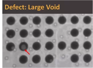
X-ray Inspection
High-energy electrons are released from the filament to excite the targThe machine releases high-energy electrons from its filament to excite a target material, generating X-rays that penetrate and reveal the sample. Due to the varying densities within the sample, the X-ray images exhibit differences in grayscale (black, white, and gray), thus indicating the location and type of defects inside the sample. X-ray inspection is a non-destructive method of sample analysis, allowing for further tests to be conducted subsequently.
Applications of X-ray inspection include:
- Observing internal defects in IC packaging components (such as wire breaks, voids, and cracks in packaging materials).
- Inspecting solder joint conditions on PCBA (including issues like voids, bridging, or the presence of solder balls).
- Analyzing the proportion of voids within solder joints.
- Viewing various materials from different angles.
- Observing the filling conditions inside porous materials.
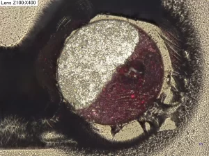
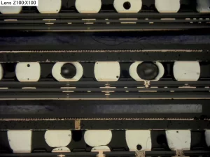
Digital Microscope
Equipped with a multi-lighting system, this device can observe at magnifications ranging from 50x to 2500x. Using visible light reflection off the surface of the object, it allows for the examination of the brightness, darkness, depth, and shallowness of the test subject. Furthermore, image capture of the sample’s surface is enhanced through the optical lens’s ability to zoom in and out. In addition to this, digital microscopes can also perform image depth composition for samples with height differences.
Therefore, this equipment is well-suited for inspecting IC packaging components (appearance, defects, discoloration), observing defects in the appearance or surface treatment of PCB boards, examining various soldering point defects in PCBA (such as solder beads, bridging, and obvious non-wetting), and for observing surface details and characteristics of various materials.
Dye and Pry Test
Through the application of special ink, various solder points on a circuit board are immersed, allowing any micro defects in the solder points to be stained by the ink. By removing the solder joints, the stained areas (indicating the micro defects of the solder points) are exposed, enabling observation of the defect size and morphology.
Consequently, this test method is suitable for observing various solder point defects on PCBA, as well as for verifying the sealing conditions of any filling or sealing materials.
Cross Section Test
After sampling the abnormal part of the specimen, the area is encapsulated using resin. Once the resin has solidified, the targeted area is ground and polished for observation. Subsequently, the prepared sample is examined using a digital microscope or Scanning Electron Microscopy (SEM).